A GPIO write on the Pi 5 is a PCIe transaction
Back to the Pi 5 hub · measured 2026-10-30
Situation
Every older Pi I’ve played with has its GPIO block inside the SoC: on the BCM2835 it’s at 0x20200000
and you poke it. Old Pi GPIO code (RPi.GPIO, /dev/mem at 0xfe200000) simply doesn’t work on a Pi 5,
and I wanted to see why on my own board, with numbers from it. The catch:
this Pi is busy running Linux for something else, so no writes, no reboots, no sudo.
Task
Map the board from Linux alone: what’s on the PCIe link, where RP1’s registers land in the CPU’s
address space, how it boots, and what it draws at idle. One script, probe.sh, that only reads, and
logs everything to text files I can quote later.
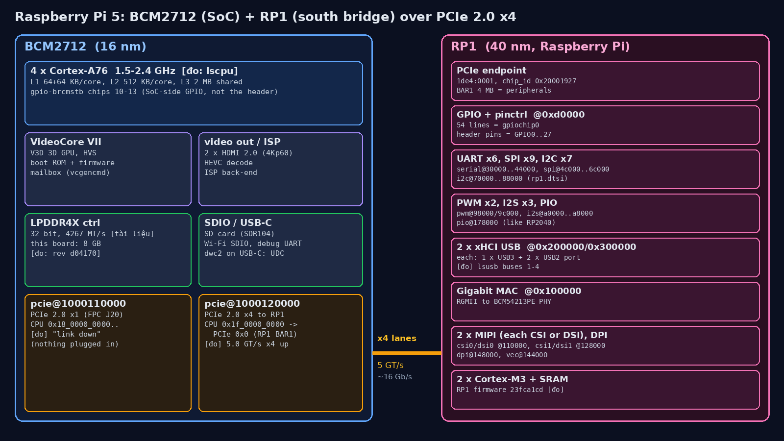 The picture I ended up with: the BCM2712 on the left, RP1 (GPIO, UART, SPI, I2C, USB, Ethernet, MIPI) on the right, four PCIe lanes at 5 GT/s between them. Addresses from this board’s device tree.
Action
What’s on PCIe. lspci shows one bridge and one device behind it, the RP1. dmesg has the link and
the windows:
[    0.960391] brcm-pcie 1000110000.pcie: link down
[    0.964334] brcm-pcie 1000120000.pcie:      MEM 0x1f00000000..0x1ffffffffb -> 0x0000000000
[    1.074372] brcm-pcie 1000120000.pcie: link up, 5.0 GT/s PCIe x4 (!SSC)
[    1.094962] rp1 0002:01:00.0: bar1 len 0x400000, start 0x1f00000000, end 0x1f003fffff, flags, 0x40200
[    1.096288] rp1 0002:01:00.0: chip_id 0x20001927
The first controller (1000110000, the external PCIe connector) is “link down”: nothing plugged in.
The second one is RP1, four lanes at 5 GT/s. Its BAR1 (4 MB) is at CPU 0x1f_0000_0000, and that window
maps to PCIe address 0x0.
Following one write. Put together with the ranges property of the rp1 node, a store to set GPIO17
(1 << 17 into the RIO0 OUT register, SET alias) goes like this:
| Seen from | Address |
|---|---|
| CPU (Cortex-A76) | 0x1f_000e_2000 |
| PCIe bus | 0x00_000e_2000, a 4-byte memory write |
| inside RP1 | 0xc0_400e_2000 (sys_rio0 + 0x2000 SET) |
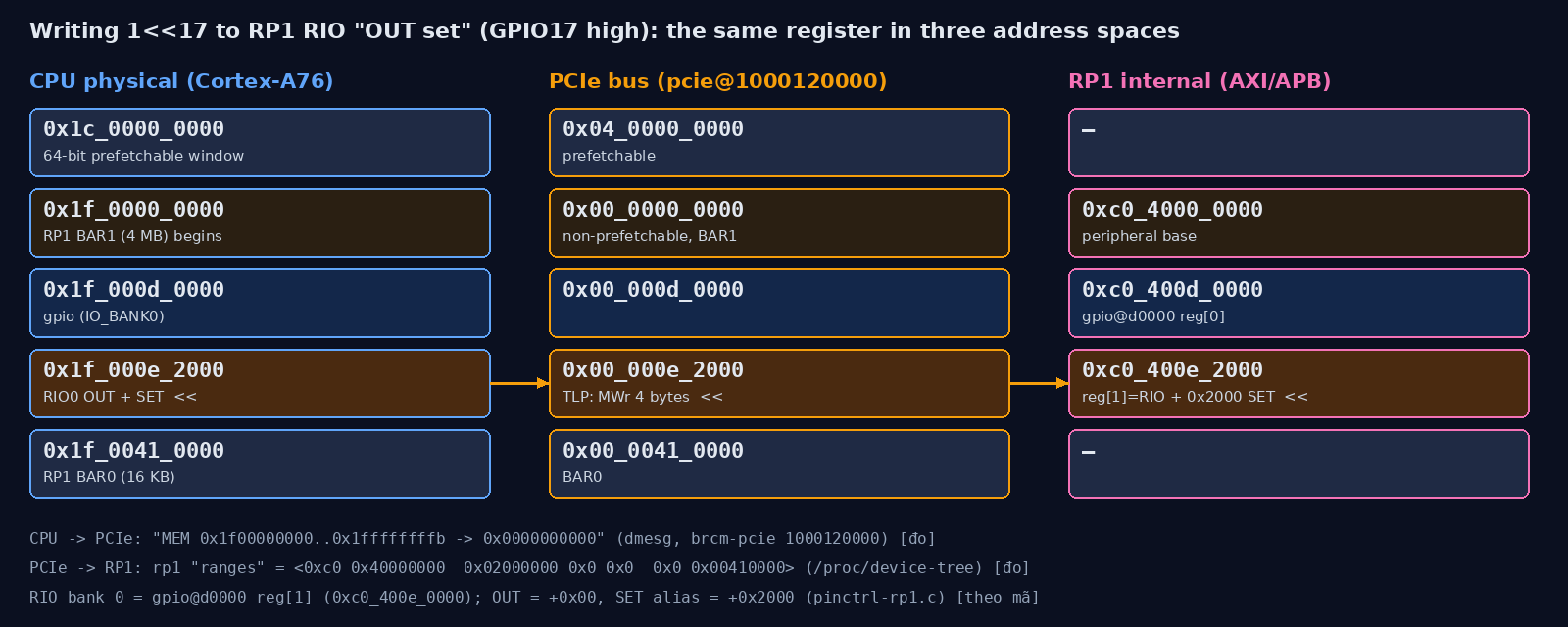 The same GPIO17 SET write in the three address spaces: CPU
0x1f_000e_2000, PCIe 0x00_000e_2000, RP1 0xc0_400e_2000.
So yes, toggling a pin is a posted write across the PCIe link to another chip. I didn’t time it; I didn’t want to toggle pins on a shared board.
Naming trap. Early Pi 5 kernels called the RP1 GPIO chip gpiochip4. On this 6.18 kernel it’s
gpiochip0:
$ gpiodetect
gpiochip0 [pinctrl-rp1] (54 lines)
gpiochip10 [gpio-brcmstb@107d508500] (32 lines)
Scripts should open it by label (pinctrl-rp1), not by number.
Boot and power. The EEPROM bootloader is the 2025/11/05 release with BOOT_ORDER=0xf461 (SD
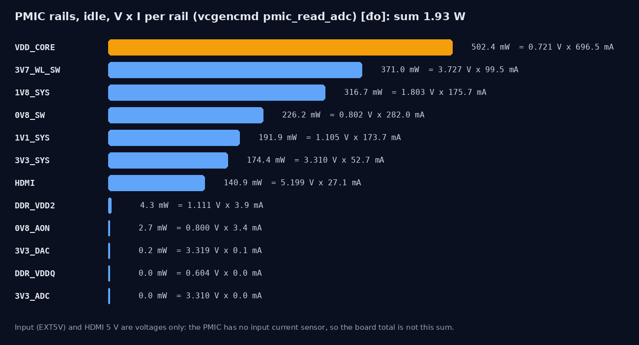
first). The PMIC reports current and voltage per rail with vcgencmd pmic_read_adc; VDD_CORE alone is
0.72 V x 0.70 A. And the USB current limit is set from what the supply says it can do:
$ vcgencmd get_config usb_max_current_enable
usb_max_current_enable=0
$ cat /proc/device-tree/chosen/power/max_current | od -An -tu4 --endian=big
       3000
A 3 A supply, not the 5 A USB-PD one, so all USB ports together are held to 600 mA (that part is from the Raspberry Pi docs). If a USB disk keeps dropping on a Pi 5, this is the first thing I’d check.
Result
RP1 sits behind PCIe x4 at 5 GT/s and its registers appear at CPU 0x1f_0000_0000, so a GPIO
write is a PCIe memory write to 0x1f_000e_2000. The RP1 GPIO chip is gpiochip0 on this kernel,
not gpiochip4, and with this 3 A supply USB is held to 600 mA total.
At idle the ARM runs at 1.5 GHz (measure_clock arm = 1500019456), 47.7 C, fan at level 0
of 4, throttled=0x0. The sum of V x I over the PMIC rails is ~1.93 W (VDD_CORE 502 mW of it).
That leaves out whatever the PMIC can’t see, so it’s not the wall power.
What I’d do next
Time a GPIO toggle with a scope once I’m allowed to touch the pins, and compare it with the BCM2835’s in-SoC GPIO. I’d expect the PCIe round trip to show up in reads (a read has to wait for RP1 to answer), much less in posted writes. That’s a guess until I measure it.