My own boot0 in NAND block 0: an LED from SRAM, then an app in DRAM
Back to the D1 Nezha hub · measured 2026-09-28
Situation
From the first day I knew the boot
ROM loads an eGON.BT0 image from the start of the SPI-NAND into SRAM and jumps to it, and that I
could get into FEL from software to put things back. On a normal boot that image is Tina’s boot0, then
OpenSBI, U-Boot, the kernel. I wanted my code to be the very first thing after the ROM.
Task
First a bare-metal program that the ROM itself loads from NAND: no boot0, no OpenSBI, no U-Boot, no DRAM, just the on-board RGB LED cycling its colours. Then a second stage in DRAM, which means doing the DDR3 training myself. And I had to be able to undo all of it.
Action
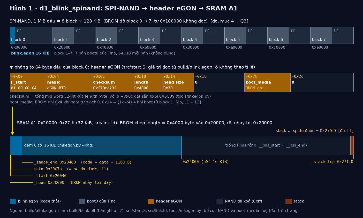
The image. start.S with the 64-byte eGON header (a jal over it, the magic, length, checksum),
a linker script for SRAM A1 at 0x20000, and a small tool (mkegon) that pads the image and computes
the checksum the same way the stock boot0’s checksum checked out. Built with zig’s clang, because a
riscv64 GCC wasn’t there. The “LED” on the Nezha turned out to be a WS2812 on PC0 driven by the LEDC
block, not a GPIO LED; I only found that by reading the Linux driver (after first downloading the
wrong path from cgit and getting a 41-line HTML page).
I tested over FEL first (xfel write + exec, no flash touched): all four colours, and the program
returned to FEL cleanly.
Backup before writing. Reading the first 1 MiB back showed something I hadn’t expected: Tina keeps
8 copies of boot0, one per 128 KiB block (0x0, 0x20000, … 0xe0000). My make flash only
erases block 0; the other 7 stay, and the ROM runs the first valid image it finds.
Flashed. I wrote block 0 and power-cycled. No ADB (Tina didn’t boot), the LED cycled, and my UART line had the proof:
boot_media=0x00000004: the ROM writes this into the header of the image it loaded, and 4 is
SPI-NAND (before that run it was only my inference from the ROM code). pc=0x2007a, which is main
in the map file, and sp=0x27f60, under my stack top. And PLL_CPU=0xfa001000: 408 MHz, the ROM’s
setting, so no boot0 ran before me.
Undo. Erasing block 0 to all ff and power-cycling: Tina came back, boot0 starting at [158]
instead of the usual [45], and the header said boot_media = 0x14, copy number 1. Exactly what the
ROM code predicted: it skipped the empty block and took the next copy. Then I restored the 1 MiB backup
and diffed it.
Second stage. SRAM A1 is 32 KB, no room for anything real. So: an SPL (24 KiB eGON.BT0) that
sets PLL_CPU to 1008 MHz, trains the DDR3 with lib-dram (the same code xfel ddr d1 uses), brings up
SPI0 at 50 MHz, reads an app header at NAND 0x10000, copies the app straight into DRAM at
0x40000000, checks it and jumps. The app checks an 8 MiB .bss array (that could never fit in SRAM)
and blinks.
 The SPL in five steps, numbers from its UART output: PLL to 1008 MHz, DDR3 trained in 51 124 us, SPI0 at 50 MHz, the app header at NAND
0x10000, jump to 0x40000000.
Result
My code runs straight from the boot ROM out of NAND: no Tina, no OpenSBI, no U-Boot. The blink
image is 1160 bytes of code and data, padded to 16 KiB. The SPL trains 1024 MiB of DDR3 in
51 124 us, reads SPI-NAND ID c226, and the app runs at pc=0x4000005a with the 8 MiB .bss
check at 0 bad words.
The ROM’s fallback is real and measured: with block 0 empty it boots copy 1 (boot_media 0x14).
And I can go back to stock any time: FEL, then make restore, and the 1 MiB readback matches the
backup.
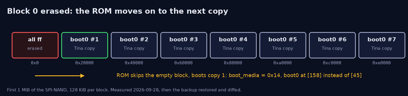 The undo test as a picture: block 0 all
ff, the ROM moves to Tina’s copy at 0x20000 and says so in the header (boot_media = 0x14).
What I’d do next
The 64 KiB app slot is now my bottleneck: the FreeRTOS image is 84 KB and doesn’t fit. Moving the app to a later block means the SPL has to skip Tina’s boot0 copies, or I give up a couple of them.